Login
Contact


 Share :
Description
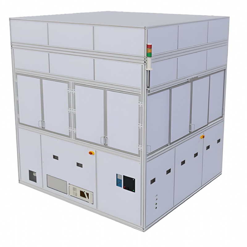
Repairing the metal circuits short defect on PCB substrate
Read the defect data from various AOI machine, and move the corresponding coordinate position to start laser repair
Precision processing (Min Spot size around 1 um)
Can correspond to circuit thickness under 25 um.
Read the defect data from various AOI machine, and move the corresponding coordinate position to start laser repair
Precision processing (Min Spot size around 1 um)
Can correspond to circuit thickness under 25 um.
Related Products
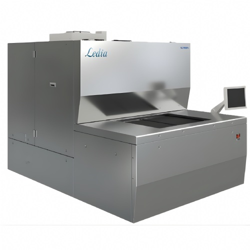
Direct Imaging System - Ledia 6S

Visual Inspection Equipment - CARIS-1100M

Direct Imaging System - Ledia 8F

Optical Inspection System (AOI) - MIYABI X/S/B/C
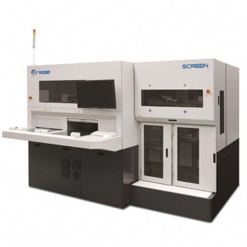
Automatic Final Visual Inspection System (AVI) - FP9200S/F/FL
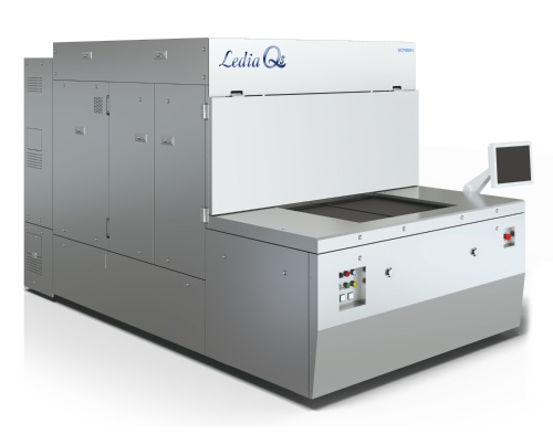
Direct Imaging System - Ledia Qs
Highest Rated Products
Back
 Product Inquiry